|
B863–032 Monitored 24 Vdc Input, Quick Start Test
|
|


|
(Original Document)
|
|
B863–032 Monitored 24 Vdc Input, Quick Start Test
|
|
|
(Original Document)
|
|
Step
|
Action
|
|---|---|
|
1
|
Stop the controller.
|
|
2
|
Determine which channel and slot location are being used for this module and insert the module.
|
|
3
|
Wire +24 Vdc external power supply to terminal 18, and connect common to terminal 20 on a AS-8535-000 high density connector. Do not connect any other field wiring to the connector.
NOTE: Remove the keying tabs on the AS-8535-000 high density connector prior to installing module. |
|
4
|
Turn ON the external 24 Vdc power supply. The Field Power light will come ON.
|
|
5
|
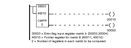
I/O Map the module as a B863, four register inputs 30001 ... 30004 binary. Recall that the first two registers are used for real inputs, and the last two registers are error flags.
|
|
6
|
Start the controller.
|
|
7
|
Confirm that the module’s active light is illuminated.
Note: Active on steady = OK. Active blinking = Check the 24 Vdc external power supply voltage and wiring.
|
|
8
|
View the B863 I/O mapped registers, 30001 ... 30004 on the reference screen in binary format.
|
|
9
|
Verify that all the points are zero.
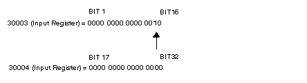
The first two registers, 30001 and 30002 are real inputs. Open inputs to the module reads 0. The second two registers, 30003 and 30004 are error flags. A value of 1 in any of these error flag points indicates a faulty input.
|
|
10
|
Turn OFF the external 24 Vdc power supply, and all error flag points change to 1.
|
|
11
|
Turn ON the external 24 Vdc power supply, and all error flag points change back to 0.
|
|
12
|
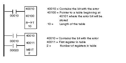
To test an input, connect a wire from the +24 Vdc point on the connector terminal 18, and touch the other end of the wire to terminal 1. Bit 1 in 30001 goes from 0 to 1. The error flag for input 1 is found at bit 1 in register 30003. When the input is functional this reads 0.
|
|
B863-032 Input 15 Error Table
|
|
|
Register
|
Data
|
|
40100
|
0001 ¨ Pointer to Table
|
|
40101
|
0015 ¨ Fault with Input Bit 15
|
|
40102
|
0000
|
|
40103
|
0000
|
|
.. .
|
.. .
|
|
40110
|
0000
|