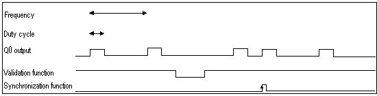
In this operating mode, the module uses an internal clock generator to supply a periodic signal at the module’s Q0 output. Only the Q0 output is concerned by this mode as the Q1 output is independent of this mode.
The output_block_0_enable command bit (%Qr.m.c.2) must be set to 1 in order to enable a modulation at the Q0 output.
The active validation function enables the operation of the internal clock generator that produces the output signal to be validated.
The active synchronization function enables the output signal to be synchronized by resetting to 0 the internal clock generator.
The wave form of the output signal depends on:
-
The pwm_frequency value (%QDr.m.c.6): it defines the frequency from 0.1 Hz (value is equal to 1) to 4 KHz (value is equal to 40,000), in increments of 0.1 Hz
-
The pwm_duty value (%QWr.m.c.8): it defines the duty cycle from 5 % (value is equal to 1) to 95 % (value is equal to 19) in increments of 5 %.
The following figure shows the operation of the module in the pulse width modulation mode:
Counter Status Bits in Pulse Width Modulation Mode
The table below shows the composition of the counter’s %IWr.m.c.0 status word in pulse width modulation mode:
|
Bit
|
Label
|
Description
|
|
%IWr.m.c.0.3
|
VALIDITY
|
Validity bit is used to indicate that the output data (frequency and duty cycle) unter current value and compare status registers contain valid data.
If the bit is set to 1, the data is valid.
If the bit is set to 0, the data is not valid.
|
|
%IWr.m.c.0.4
|
HIGH_LIMIT
|
The output frequency or the duty cycle is out of range (high limit).
|
|
%IWr.m.c.0.5
|
LOW_LIMIT
|
The output frequency or the duty cycle is out of range (low limit).
|
In this mode, the type of the IODDT must be T_UNSIGNED_CPT_BMX.
The maximum output frequency is 4 kHz.
The maximum frequency that can be applied to the IN_SYNC input is 1 pulse every 5 ms.
The Q0 driver is "source type", therefore a load resistance is required to switch the output signal Q0 to 0 V using the correct frequency. We recommend a load resistance of 250 Ω.
The allowed duty cycle varies according to the frequency of the Q0 output.
The table below shows duty cycle values according to the selected frequency. These values must be observed for normal operation:
|
Frequency
|
Duty cycle
|
|
0.1... 250 Hz
|
95% - 5%
|
|
251... 500 Hz
|
90% - 10%
|
|
501... 1 000 Hz
|
80% - 20%
|
|
1001... 1 500 Hz
|
70% - 30%
|
|
1501... 2 000 Hz
|
60% - 40%
|
|
2 001... 2 500 Hz
|
50%
|
|
2 5001... 4 000 Hz
|
50% (See following note )
|
NOTE: If the frequency and the duty cycle do not respect this table, the output and the validity bit (%IWr.m.c.0.3) remains in the low state.
NOTE: You have to check the validity bit (%IWr.m.c.0.3) before taking into account the numerical values such as the counter and the capture registers. Only the validity bit at the high level (set to 1) guarantees that the mode will operate correctly within the limits.
NOTE: From 2501 Hz to 4000 Hz, the 50% ratio is not guaranteed on output.